AMD Instinct™ MI250 microarchitecture#
2025-10-30
7 min read time
The microarchitecture of the AMD Instinct MI250 GPU is based on the AMD CDNA 2 architecture that targets compute applications such as HPC, artificial intelligence (AI), and machine learning (ML) and that run on everything from individual servers to the world’s largest exascale supercomputers. The overall system architecture is designed for extreme scalability and compute performance.
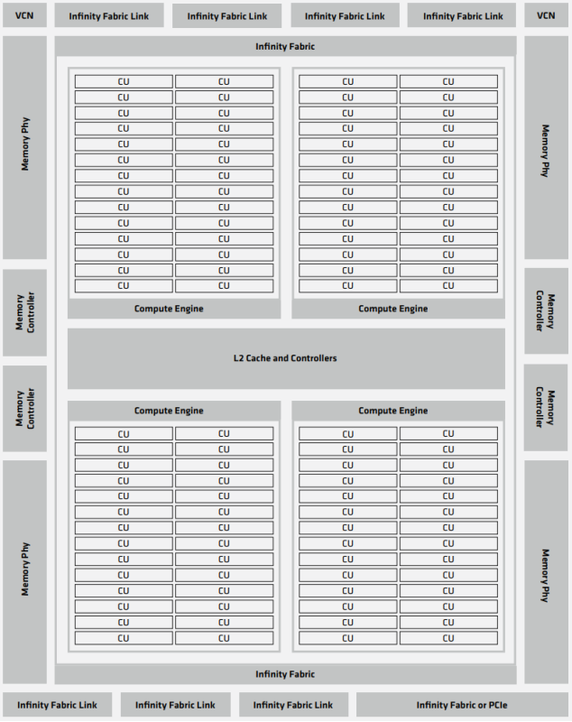
The following image shows the components of a single Graphics Compute Die (GCD) of the CDNA 2 architecture. On the top and the bottom are AMD Infinity Fabric™ interfaces and their physical links that are used to connect the GPU die to the other system-level components of the node (see also Section 2.2). Both interfaces can drive four AMD Infinity Fabric links. One of the AMD Infinity Fabric links of the controller at the bottom can be configured as a PCIe link. Each of the AMD Infinity Fabric links between GPUs can run at up to 25 GT/sec, which correlates to a peak transfer bandwidth of 50 GB/sec for a 16-wide link ( two bytes per transaction). Section 2.2 has more details on the number of AMD Infinity Fabric links and the resulting transfer rates between the system-level components.
To the left and the right are memory controllers that attach the High Bandwidth Memory (HBM) modules to the GCD. AMD Instinct MI250 GPUs use HBM2e, which offers a peak memory bandwidth of 1.6 TB/sec per GCD.
The execution units of the GPU are depicted in the following image as Compute Units (CU). The MI250 GCD has 104 active CUs. Each compute unit is further subdivided into four SIMD units that process SIMD instructions of 16 data elements per instruction (for the FP64 data type). This enables the CU to process 64 work items (a so-called “wavefront”) at a peak clock frequency of 1.7 GHz. Therefore, the theoretical maximum FP64 peak performance per GCD is 22.6 TFLOPS for vector instructions. This equates to 45.3 TFLOPS for vector instructions for both GCDs together. The MI250 compute units also provide specialized execution units (also called matrix cores), which are geared toward executing matrix operations like matrix-matrix multiplications. For FP64, the peak performance of these units amounts to 90.5 TFLOPS.
Computation and Data Type |
FLOPS/CLOCK/CU |
Peak TFLOPS |
|---|---|---|
Matrix FP64 |
256 |
90.5 |
Vector FP64 |
128 |
45.3 |
Matrix FP32 |
256 |
90.5 |
Packed FP32 |
256 |
90.5 |
Vector FP32 |
128 |
45.3 |
Matrix FP16 |
1024 |
362.1 |
Matrix BF16 |
1024 |
362.1 |
Matrix INT8 |
1024 |
362.1 |
The above table summarizes the aggregated peak performance of the AMD Instinct MI250 Open Compute Platform (OCP) Open Accelerator Modules (OAMs) and its two GCDs for different data types and execution units. The middle column lists the peak performance (number of data elements processed in a single instruction) of a single compute unit if a SIMD (or matrix) instruction is being retired in each clock cycle. The third column lists the theoretical peak performance of the OAM module. The theoretical aggregated peak memory bandwidth of the GPU is 3.2 TB/sec (1.6 TB/sec per GCD).
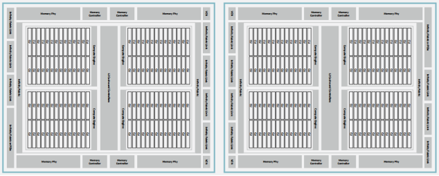
The following image shows the block diagram of an OAM package that consists of two GCDs, each of which constitutes one GPU device in the system. The two GCDs in the package are connected via four AMD Infinity Fabric links running at a theoretical peak rate of 25 GT/sec, giving 200 GB/sec peak transfer bandwidth between the two GCDs of an OAM, or a bidirectional peak transfer bandwidth of 400 GB/sec for the same.
Node-level architecture#
The following image shows the node-level architecture of a system that is based on the AMD Instinct MI250 GPU. The MI250 OAMs attach to the host system via PCIe Gen 4 x16 links (yellow lines). Each GCD maintains its own PCIe x16 link to the host part of the system. Depending on the server platform, the GCD can attach to the AMD EPYC processor directly or via an optional PCIe switch . Note that some platforms may offer an x8 interface to the GCDs, which reduces the available host-to-GPU bandwidth.
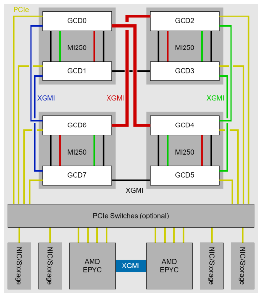
The preceding image shows the node-level architecture of a system with AMD EPYC processors in a dual-socket configuration and four AMD Instinct MI250 GPUs. The MI250 OAMs attach to the host processors system via PCIe Gen 4 x16 links (yellow lines). Depending on the system design, a PCIe switch may exist to make more PCIe lanes available for additional components like network interfaces and/or storage devices. Each GCD maintains its own PCIe x16 link to the host part of the system or to the PCIe switch. Please note, some platforms may offer an x8 interface to the GCDs, which will reduce the available host-to-GPU bandwidth.
Between the OAMs and their respective GCDs, a peer-to-peer (P2P) network allows for direct data exchange between the GPU dies via AMD Infinity Fabric links ( black, green, and red lines). Each of these 16-wide links connects to one of the two GPU dies in the MI250 OAM and operates at 25 GT/sec, which corresponds to a theoretical peak transfer rate of 50 GB/sec per link (or 100 GB/sec bidirectional peak transfer bandwidth). The GCD pairs 2 and 6 as well as GCDs 0 and 4 connect via two XGMI links, which is indicated by the thicker red line in the preceding image.